
 is excited in the STM junction by tunnelling electrons (e–). The emitted light (hν) shows a modulated spectrum resulting from a Fabry–Pérot interference of the propagating surface plasmon polariton on the shaft. Credit: Takashi Kumagai")
Spatial resolution of optical microscopy and spectroscopy is determined by how much one can confine light in space, which is usually restricted to about half-micrometre at the best due to the diffraction limit. However, light can be confined into nanometre scale by using metallic nanostructures through excitation of localised surface plasmon resonance (LSPR). Having such “nanolight” at a sharp metallic tip is particularly useful because it can be used in scanning tunnelling luminescence (STL) and scattering-type scanning near-field optical microscopy (s-SNOM) performing nanoscale imaging and spectroscopy to look at nanomaterials and even single molecules. However, precise manipulation of nanolight in nanoscale junction has remained an outstanding problem. Because the nature of nanolight (LSPR) is determined by the nanoscopic structure of the tip, its manipulation requires a fine processing technique at the nanoscale. In addition, nanolight confined into nanocavities is of key importance due to the strong enhancement effect of an electromagnetic field, which enables ultrasensitive nanoscale imaging and spectroscopy.
A research team at the Fritz-Haber Institute in Berlin, headed by Dr Takashi Kumagai, has demonstrated that manipulation of nanolight spectrum can be attained by shaping accurately plasmonic gold tips with a focused ion beam (FIB) milling technique. As a demonstration, they produced a very sharp tip with a single groove on its shaft as shown in the scanning electron microscope picture. The spectral response of nanolight confined in the nanocavity formed by the grooved tip and an atomically flat silver surface was investigated by using STL that is the combination of electronic and optical spectroscopies using scanning tunnelling microscopy. The STML spectra with the grooved tips exhibit a characteristic modulation resulting from Fabry–Pérot type interference of surface plasmon polaritons (SPPs) on the tip shaft as the standing wave formation is visualised in the electrodynamic simulation. The spectral modulation can be precisely controlled by the groove position on the shaft. They also demonstrated that the SPP Fabry–Pérot interference can be improved by optimising the overall tip shape.
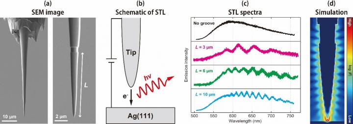
(a) SEM images of a gold FIB-tip. A single groove is made at a distance (L) from the apex. (b) Schematic of STL measurement. Light emission (hν) occurs through excitation of LSPR in the junction by tunneling electrons (e–). (c) STL spectra obtained by FIB-tips. Spectral modulation is observed for the tips with a groove and the oscillation period depends on the groove distance. (d) Electrodynamic simulations of two-dimensional electric field mapping for the FIB-tip with a groove. Standing formation of SPP occurs on the tip shaft. Credit: Takashi Kumagai
This work shows the potential of the combination of scanning probe techniques and nano-fabrication of plasmonic tips using FIB in order to study the nature of nanolight and light–matter interactions in nanocavities, which are an important frontier of plasmonics and nanooptics. In addition, the FIB-fabricated plasmonic tips are generally applicable to s-SNOM techniques, thus paving the way for nanoscale imaging and spectroscopy with a high degree of accuracy. Moreover, spectral control of the intense near-field at the apex of plasmonic tips may open up new opportunities for the realisation of coherent laser-triggered electron point sources for low-energy electron microscopy and holography techniques.
The work is reported in Nano Letters.

 located just 3 m from the exit nozzle of the engine. The testing facility is at the Instituto Nacional de Tecnica Aeroespacial (INTA) in Madrid. Credit: Gordon Humphries, University of Strathclyde")


 nano-DESI mass spectrometry imaging of liver tissue from orally dosed rat (Animal 3). a) optical image of a blood vessel within liver tissue. b) Composite ion image of charge-reduced haeme-bound α-globin (7+ and 6+ charge states; m/z 2259.9 and m/z 2636.3 respectively, red) and the charged-reduced [FABP+bezafibrate] complex (7+ and 6+ charge states; m/z 2097.5 and m/z 2446.9 respectively, blue). c) Ion image composed from charge-reduced haeme-bound α-globin (7+ and 6+ charge states) showing abundance in blood vessels. d) Ion image composed from charge-reduced [FABP+bezafibrate] complex (7+ and 6+ charge states) showing abundance in bulk tissue and absence in the blood vessel. Reproduced from https://doi.org/10.1002/ange.202202075 under a CC BY licence.")