Thomas Schmid,a Norbert Schäferb and Daniel Abou-Rasb
aFederal Institute for Materials Research and Testing, Richard-Willstätter-Str. 11, 12489 Berlin, Germany.
E-mail: [email protected]
bHelmholtz-Zentrum Berlin für Materialien und Energie GmbH, Hahn-Meitner-Platz 1, 14109 Berlin, Germany
Introduction
This overview article provides insight into how to apply Raman spectroscopy in combination with a confocal, optical microscope setup on polycrystalline material systems, in order to obtain quantitative information on phase distribution, grain sizes, crystal orientations and microstrain. Although the present work uses Cu(In,Ga)(S,Se)2 absorber layers in corresponding thin-film solar cells as a model system to demonstrate the capabilities of Raman microspectroscopy, the approaches discussed may be applied to any organic or inorganic, polycrystalline materials system.
Raman spectroscopy is an analytical tool, which may be used for the characterisation of organic and inorganic materials. By delivering very characteristic sets of frequencies of molecular or crystal lattice vibrations, this method provides access to spectroscopic “fingerprints”, which—by comparison with reference spectra—enable the identification of the chemical components of materials. Beyond this application, by evaluation of relative band intensities and exact band positions, further material properties, such as crystal orientations and stress/strain can be derived from Raman spectra.
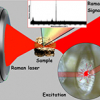
Raman spectroscopy is based on excitation by an intense and monochromatic light source (typically, a continuous, visible laser). Upon inelastic scattering of light by the material under investigation, photons with slightly shifted frequencies are generated. The frequency differences between the excitation laser light and scattered light equal the frequencies of Raman-active crystal lattice or molecular vibrations. These frequency differences are termed “Raman shifts” and are expressed in wavenumber shifts (D cm–1) see, for example, Raman spectra in Figure 1b). The collected Raman-scattered light is typically dispersed within a grating spectrometer, and spectra are detected using a charge-coupled device (CCD) camera. Thus, the whole Raman spectrum can be collected in one shot without the need of scanning, neither the excitation wavelength nor the spectrometer grating.1,2
The use of visible laser light for the excitation makes the combination of Raman spectroscopy with microscopes straightforward. In a Raman microscope, an objective lens is used for both focusing of the laser beam and collection of the light backscattered by the sample. Typically, microscopic observation enables the choice of measurement spots on the sample surface, while software-controlled, sample-scanning stages enable mapping experiments, in which in every pixel of a two-dimensional image the whole Raman spectrum (consisting of intensity and Raman-shift axes) is collected. Data analysis software enables conversion of this four-dimensional data into two-dimensional, colour-coded maps of, for example, selected band intensities that are spectroscopic images of the sample surfaces representing distributions of either chemical components or further material properties.3
Even though providing the same wavenumbers of molecular vibrations as infrared spectroscopy/microscopy, Raman microscopy has several advantages. Amongst them, the higher spatial resolution is crucial for microspectroscopic imaging. As the spatial resolution of a microscope depends linearly on the excitation wavelength, infrared microscopy has resolutions on the order of tens of micrometres, whereas Raman microscopy provides access to the submicrometre range.4 Perpendicular to the surface, the resolution in transparent samples is typically of the order of tens of micrometres, but can be tuned down to a few micrometres by the use of confocal optics. In opaque samples, depth resolution is determined by the optical penetration depth. In the strongly absorbing solar cell materials described in this article, the lateral spatial resolutions were around 400–500 nm, while perpendicular to the surface, only the top 100 nm of the thin-film samples contributed to the Raman spectra.5
The present work gives an overview of our studies on Raman microscopy in the field of thin-film solar cell research, ranging from classical Raman maps revealing the distributions of chemical constituents, via polymorphic forms and changes in stoichiometry to crystal-orientation distribution, and finally to stress/strain maps with high pixel numbers. We expect that beyond thin-film solar cell materials, the approaches presented below can be applied also on any organic or inorganic, polycrystalline material system.
Chemical composition maps and line scans
Classical approaches to analyse Raman mapping data are: (1) the identification of sample components by comparison of their spectra with reference data, (2) the definition of marker bands, which are characteristic for individual components and which do not overlap with signals from other compounds (see, for example, Figure 1b) and (3) the plot of two-dimensional distributions of (most often baseline-corrected) marker band intensities yielding spectroscopic/chemical images of the sample surface (see Figure 1c). A corresponding study was conducted on CuInS2 thin films in completed solar cell stacks prepared in cross-sectional geometry, which set the starting point of the authors’ interdisciplinary collaboration and nicely demonstrated how Raman microscopy can extend the analytical possibilities of electron microscopy in the field of thin-film solar cell research (Figure 1). Indeed, while Raman microscopy cannot compete with electron microscopy in terms of spatial resolution, the chemical information contained in Raman spectra is complementary and can be combined with elemental analysis data provided by energy-dispersive X-ray spectroscopy scanning electron microscopy (SEM–EDX).6

Figure 1. SEM image and Raman map of a cross-sectional sample of a CuInS2 solar cell stack. (a) SEM image showing well-crystallised and layered CuInS2; (b) selected Raman spectra of such a sample showing marker bands of (1) chalcopyrite CuInS2 (CH CIS), (2) CuAu I-type/disordered CuInS2 (CA CIS), (2+3) amorphous/nanocrystalline carbon and (4) copper sulfide (CuxSy); and (c) Raman map showing CH CIS (red), CA CIS (green), nanocrystalline/amorphous carbon (white), CuxSy (yellow) and the epoxy glue used to prepare the sample by the face-to-face method (blue). Adapted and extended from Reference 6.
In CuInS2 samples prepared by the spray ion layer gas reaction (ILGAR) method, SEM–EDX analysis revealed the solar cell absorber material to be present in a well-crystallised and in a layered form, consisting of alternating nanometre-thin layers of CuInS2 and carbon (Figure 1a). Raman microscopy of cross-sectional samples showed that both forms correspond to two different polymorphs of the material: the well-crystallised chalcopyrite CuInS2 and the layered CuAu I-type/disordered CuInS2 modification (Figures 1b and 1c). Furthermore, Raman microscopy identified the carbon layers as amorphous or nanocrystalline carbon and found crystals of the segregate CuxSy (formed together with In2O3 instead of CuInS2) close to chalcopyrite CuInS2 crystals. Thus, as an extension of elemental analysis by SEM–EDX, Raman microscopy can provide information on crystalline, amorphous and polymorphic phases, and their distributions.6
A more advanced way to analyse Raman data was applied in a study on cross-sectional samples of Cu(In,Ga)Se2 (CIGSe) layers prepared from solar cell stacks.7 The analysis of band-position shifts on the order of 10 cm–1 provided access to the Ga concentration gradients present perpendicular to the substrate in such layers. Varying the Ga concentration (x) in CuIn1 – xGaxSe2 thin films (ranging from CuInSe2 with x = 0 to CuGaSe2 with x = 1) leads to shifts of the most prominent (A1) mode in the Raman spectra between 173 cm–1 and 183 cm–1 due to corresponding changes of the crystal lattice constants.8 By analysing exact band positions in the Raman spectra collected at high spectral resolution (approximately 0.4 cm–1/CCD pixel), Ga concentration gradients were calculated from these spectra, which were in good agreement with results obtained by various other methods for elemental distribution analysis,7 including also Raman depth profiling being realised by alternating sputtering of a crater and acquisition of Raman spectra within the crater.9

Figure 2. Measurement of Ga concentration gradients in Cu(In,Ga)Se2. (a) Raman spectra measured across a Cu(In,Ga)Se2 layer in a cross-sectional solar stack sample starting from the surface (0 µm) towards the molybdenum back contact; (b) Raman shifts of the most prominent mode (A12 and calculated relative Ga concentrations; and (c) Raman intensity of the most prominent MoSe2 band normalised to the Cu(In,Ga)Se2 A1 mode intensity as a measure for the steeply increasing MoSe2 concentration towards the molybdenum back contact. Adapted and extended from Reference 7.

Figure 3. Three Raman spectra (black, violet and blue lines) from various points in CuInSe2 thin films, highlighting the contained microstructural information. The Raman modes can be assigned to different crystal lattice vibrations of CuInSe2 (labelled A1, E and B2+E). Plotting relative band intensities (e.g. the A1 mode in red and B2+E mode in green) yields crystal distribution-orientation maps, whereas small shifts of Raman bands as image contrast reveal distributions of stress and strain. The same red, green and blue colour codes are used in Figures 4 and 5 as well. Adapted from Reference 5.
Orientation-distribution and strain maps
Since the early years of Raman spectroscopy the effect of crystal orientation on Raman intensities has been known.10 Mathematically, the Raman intensity depends on the polarisability tensor of the crystal or molecule under investigation and the three-dimensional orientation of the polarisation of the beam of light employed for excitation; in very simple words, the intensities of the individual vibrational modes of a material depend on the efficiency of their excitation by the incoming light waves. The excitation is very efficient if the polarisation direction of the light is parallel to the main direction of a vibrational motion and becomes very inefficient with perpendicular orientation. This effect was previously demonstrated using single crystals of CuInSe2,11 while we applied Raman spectroscopy on polycrystalline CuInSe2 thin films as a model system in our study.
We found that the relative intensity changes of the A1 mode (marked red in Figure 3) and the B2+E mode (marked green in Figure 3) of CuInSe2 can be used as contrasts in mapping experiments to reveal individual crystals of polycrystalline surfaces of this material. The main advances of our approach are the high pixel numbers, the evidence by means of another independent method that basically all crystals (down to submicrometre scales) can be visualised by the approach, and the good agreement with theoretical predictions revealing the quantitative character of the measurement.5
In our study, typical maps with high pixel numbers consisted of 200 × 200 pixels (or 40,000 individual Raman spectra) with step sizes of 250 nm, thereby covering an area of 50 ×50 µm2. By oversampling, we make use of the full lateral spatial resolution of Raman microspectroscopic imaging, which we demonstrated to be approximately 400 nm at 632.8 nm laser excitation through a microscope objective lens with 100× / NA = 0.90. Figure 4 shows a large Raman map collected on the same area on which also an electron backscatter diffraction (EBSD) map was acquired. The Raman map consists of the superimposed spatial intensity distributions of the two selected Raman modes (red and green). The good agreement of the EBSD and Raman intensity maps is obvious, and basically all crystals with sizes above the resolution limit of Raman microscopy are visible in both images. Indeed, while Raman microscopy cannot compete with EBSD in terms of spatial resolution, its main advantage in this context is the ease of the approach. Since basically all samples which can be used for light microscopy are also compatible with Raman microscopy, in most cases, no or only very little additional sample preparation is needed. Compared with the extensive preparation and analysis efforts necessary for EBSD, this means there is no need for polishing, coating with conductive material or transfer to high vacuum.
Another interesting feature of Raman mapping analyses of polycrystalline materials is the possibility to evaluate small band shifts for assessment of stress and strain. In a stressed crystal the crystal lattice constants are slightly smaller than in the equilibrium state resulting in higher vibrational frequencies. As the observed shifts of the A1 mode of CuInSe2 were typically within 1 cm–1, only three to four steps of approximately 0.3 cm–1 (defined by the spectral resolution of the instrument) were detected when analysing the raw data. As described in a recent report, the resolution can be improved to 0.05 cm–1 by peak fitting using a Lorentzian or Gaussian distribution.12 Fitting each of the 40,000 peaks with a Gaussian resulted in the Raman image shown in Figure 4c.
Raman shifts can be converted into stress in GPa based on experimentally determined, material-dependent conversion factors (CuInSe2: 5 cm–1/GPa),13,14 which in turn yields strain as the ratio of stress and the Young’s modulus (CuInSe2: 68.8 GPa).15 A more detailed description of this procedure can be found in Reference 16. Indeed, the microstrain values were measured on the exactly same sample area as the orientation-distribution map because they were extracted from the same spectra just by evaluating band shifts instead of band intensities (see Figure 3). Microstrain values measured within individual grains in polycrystalline CuInSe2 thin films were all on the order of 10–4. Comparison with the microstrain values determined by EBSD and X-ray microdiffraction16,17 showed good agreement with the Raman data, underlining the quantitative character of the approach. However, while EBSD and X-ray microdiffraction were also able to provide decent distributions of microstrain within individual grains with spatial resolution well below 100 nm, the sensitivity of the microstrain measurement (i.e., the capability to distinguish microstrain values of neighbouring measurement points) using Raman microspectroscopy for the given microstrain values of only 10–4 was not sufficient.

Figure 4. Crystal-orientation maps based on (a) relative Raman intensities of the A1 (green) and B2+E modes (red) and on (b) EBSD measurement of the same identical position within the sample. (c) Evaluation of A1 Raman band positions revealing stress and strain. The white rectangle relates to Figure 5. Adapted and extended from Reference 5.
The question as to whether also the crystal orientation data contains quantitative information was solved by comparison of experimental Raman data with theoretical predictions. Figure 5 shows Raman maps, which were performed on the area marked with a white rectangle in Figure 4. Two different laser polarisation directions reveal very different behaviour of the two selected Raman modes (Figures 4a and 4b). The crystal planes exposed to the sample surface were determined from EBSD data for individual crystallites (Figure 4c). Examples for two grains are shown in Figures 4d and 4e. For the determined crystal planes, theoretical modelling predicted the behaviour of the two Raman modes as a function of polarisation angle. The experimental data for the two polarisation directions shown in Figures 4a and 4b matched well the theoretical prediction.5 We expect that measurements with several (not only two) polarisation directions can reveal characteristic profiles of Raman intensities, from which quantitative information on crystal planes and orientations can be derived.
Conclusions
We have demonstrated that Raman microspectroscopic imaging of polycrystalline materials can reveal
- distributions of molecules and solid phases,
- polymorphic and amorphous phases,
- gradual changes of stoichiometries,
- the individual crystallites in polycrystalline material surfaces,
- quantitative information on crystal orientation and
- quantitative information on stress and strain.
Even though with lateral resolutions on the order of 500 nm, it will never be able to compete with electron-microscopy-based approaches, an important advantage of Raman microspectroscopy is the ease of its application, as in many cases no or very little sample preparation is needed and the experiments are performed at atmospheric pressure.

Figure 5. Raman microscopy and EBSD maps of the area marked with a white rectangle in Figure 4. (a) Raman intensity map with laser polarisation direction parallel to the x axis of the image (same direction as in Figure 4); (b) Raman intensity map acquired with laser polarisation direction rotated by 90°; (c) EBSD map; and (d, e) representations of the crystal planes resembling grains 1 and 2 in (c) as determined from EBSD data. Adapted and extended from Reference 5.
References
- R.L. McCreery, Raman Spectroscopy for Chemical Analysis. Wiley (2000). doi: http://dx.doi.org/10.1002/0471721646
- P. Vandenabeele, Practical Raman Spectroscopy: An Introduction. Wiley (2013). doi: http://dx.doi.org/10.1002/9781119961284
- L. Opilik, T. Schmid and R. Zenobi, “Modern Raman imaging: vibrational spectroscopy on the micrometer and nanometer scales”, Ann. Rev. Anal. Chem. 6, 379–398 (2013). doi: http://dx.doi.org/10.1146/annurev-anchem-062012-092646
- J. Álvarez-García, V. Izquierdo-Roca, P. Pistor, T. Schmid and A. Pérez-Rodríguez, “Raman spectroscopy on thin films for solar cells”, in Advanced Characterization Techniques for Thin Film Solar Cells (2nd Edition), Ed by D. Abou-Ras, T. Kirchartz and U. Rau. Wiley, Ch. 17, pp. 469–499 (2016). doi: http://dx.doi.org/10.1002/9783527699025.ch17
- T. Schmid, N. Schäfer, S. Levcenco, T. Rissom and D. Abou-Ras, “Orientation-distribution mapping of polycrystalline materials by Raman microspectroscopy”, Sci. Rep. 5, 18410 (2015). doi: http://dx.doi.org/10.1038/srep18410
- T. Schmid, C. Camus, S. Lehmann, D. Abou-Ras, Ch.-H. Fischer, M.C. Lux-Steiner and R. Zenobi,” Spatially resolved characterization of chemical species and crystal structures in CuInS2 and CuGaxSey thin films using Raman microscopy”, Phys. Status Solidi A 206, 1013–1016 (2009). doi: http://dx.doi.org/10.1002/pssa.200881156
- D. Abou-Ras, R. Caballero, C.H. Fischer, C.A. Kaufmann, I. Lauermann, R. Mainz, H. Mönig, A. Schöpke, C. Stephan, C. Streeck, S. Schorr, A. Eicke, M. Döbeli, B. Gade, J. Hinrichs, T. Nunney, H. Dijkstra, V. Hoffmann, D. Klemm, V. Efimova, A. Bergmaier, G. Dollinger, T. Wirth, W. Unger, A.A. Rockett, A. Perez-Rodriguez, J. Alvarez-Garcia, V. Izquierdo-Roca, T. Schmid, P.P. Choi, M. Müller, F. Bertram, J. Christen, H. Khatri, R.W. Collins, S. Marsillac and I. Kötschau, “Comprehensive comparison of various techniques for the analysis of elemental distributions in thin films”, Microsc. Microanal. 17, 728–751 (2011). doi: http://dx.doi.org/10.1017/S1431927611000523
- C. Rincón and F.J. Ramírez, “Lattice vibrations of CulnSe2 and CuGaSe2 by Raman microspectrometry”, J. Appl. Phys. 72, 4321–4324 (1992). doi: http://dx.doi.org/10.1063/1.352195
- X. Fontané, V. Izquierdo-Roca, L. Calvo-Barrio, A. Pérez-Rodríguez, J.R. Morante, D. Guettler, A. Eicke and A.N. Tiwari, “Investigation of compositional inhomogeneities in complex polycrystalline Cu(In,Ga)Se2 layers for solar cells”, Appl. Phys. Lett. 95, 261912 (2009). doi: http://dx.doi.org/10.1063/1.3280049
- S. Bhagavantam, “Effect of crystal orientation on the Raman spectrum of calcite”, Proc. Ind. Acad. Soc. A 11, 62–71 (1940).
- H. Tanino, H. Fujikake, T. Maeda and H. Nakanishi, “Determination of the crystal orientation of CuInSe2 by Raman spectroscopy”, J. Appl. Phys. 74, 2114–2116 (1993). doi: http://dx.doi.org/10.1063/1.354735
- M. Becker, H. Scheel, S. Christiansen and H.P. Strunk, “Grain orientation, texture, and internal stress optically evaluated by micro-Raman spectroscopy”, J. Appl. Phys. 101, 063531 (2007). doi: http://dx.doi.org/10.1063/1.2434961
- H. Tanino, T. Maeda, H. Fujikake, H. Nakanishi, S. Endo and T. Irie, “Raman spectra of CuInSe2”, Phys. Rev. B 45, 13323–13330 (1992). doi: http://dx.doi.org/10.1103/PhysRevB.45.13323
- J. González, M. Quintero and C. Rincón, “Pressure dependence of the Raman A1 mode and pressure-induced phase transition in CuInSe2”, Phys. Rev. B 45, 7022–7025 (1992). doi: http://dx.doi.org/10.1103/PhysRevB.45.7022
- L.I. Berger, Semiconductor Materials. CRC Press (1997).
- N. Schäfer, A.J. Wilkinson, T. Schmid, A. Winkelmann, G.A. Chahine, T.U. Schülli, T. Rissom, J. Marquardt, S. Schorr and D. Abou-Ras, “Microstrain distribution mapping on CuInSe2 thin films by means of electron backscatter diffraction, X-ray diffraction, and Raman microspectroscopy”, Ultramicroscopy 169, 89–97 (2016). doi: http://dx.doi.org/10.1016/j.ultramic.2016.07.001
- N. Schäfer, G.A. Chahine, A.J. Wilkinson, T. Schmid, T. Rissom, T.U. Schülli and D. Abou-Ras, “Microstrain distributions in polycrystalline thin films measured by X-ray microdiffraction”, J. Appl. Crystallogr. 49, 632–635 (2016). doi: http://dx.doi.org/10.1107/S1600576716003204