Andrew J. Pollard and Debdulal Roy
National Physical Laboratory, Hampton Road, Teddington, Middlesex TW11 0LW, United Kingdom.
E-mail: [email protected]
Introduction
Graphene, a two-dimensional material consisting of carbon atoms in a honeycomb lattice, is transitioning from academic curiosity to commercial product, since its first isolation over a decade ago. The reasons for this rapid advancement are the exciting properties of this nanomaterial. Graphene has been shown to have amazing electrical mobility, thermal conductivity and is the strongest material ever tested.1 Within the scientific community, other two-dimensional (2D) materials are now also being investigated, such as boron nitride, molybdenum disulfide, tungsten diselenide and combinations of these materials in stacked heterostructure configurations.2 The many different types of 2D material now being researched provide an atomic-level tool-box, from which the type of material required, for example a semimetal, semiconductor, insulator or superconductor, can be chosen. However, the level of scientific understanding of these materials is not as advanced as for graphene and therefore these other 2D materials have not yet started to enter the commercial sector.
There are now hundreds of companies worldwide claiming the commercial production of graphene, with the graphene market estimated to be €17.5 million in 2014.3 There are also many industry areas that are predicted to be disrupted by graphene, such as flexible electronics, additive manufacturing, optoelectronics, sensors, composites, barriers and energy storage.4 Several companies have even announced graphene products, such as sporting goods, batteries and mobile phones. However, the characterisation of graphene produced on the large-scale and included within real-world products will be extremely important for the development of this emerging technology and to instil industrial confidence. Accurate, reliable and standardised characterisation could provide the confidence that graphene-product claims are real and graphene is actually present, as well as determining whether the material included is graphene rather than graphite, the three-dimensional (3D) counterpart of graphene. Beyond these issues, the measurement of the actual properties of the graphene material, such as structural dimensions, level of disorder and level of oxygen content, will be required for the advancement and development of graphene and graphene products.
Raman spectroscopy has been shown to be a particularly effective tool for probing carbon materials for several decades, but more recently for carbon nanostructures such as carbon nanotubes, the one-dimensional (1D) allotrope of carbon. It is therefore of no surprise that a large amount of scientific research has been performed using Raman spectroscopy to measure many of the properties of the 2D allotrope of carbon, graphene. As a rapid and non-destructive optical characterisation technique, the possibilities of Raman spectroscopy being used as part of any quality control system for the large-scale industrial production of graphene are apparent. This is enforced by the realisation that this technique can be used to understand the number of layers, strain, doping and importantly the level of disorder present in graphene.5
Graphene defects
As graphene is a nanoscale material, the measurement of its properties is particularly challenging, as is the characterisation of defects in graphene, such as a “vacancy defect”, which is the absence of a carbon atom (or several atoms) from the hexagonal graphene lattice. Meanwhile, the effect of graphene defects on the properties of graphene have been extensively investigated, but the effect is not always negative. Whilst not desired for typical electronic devices due to the reduction in electrical conductivity, for the desalinisation of water, vacancy defects would be required. Similarly, “sp3 bonded adatom defects” in graphene, where other non-carbon atoms or species are bound to the graphene basal plane, would be necessary for sensing applications to enable sensor selectivity. Raman spectroscopy is highly desirable for the characterisation of graphene in commercial applications, since it can provide an insight into the level of disorder in graphene quickly (and if performed correctly, without increasing the number of defects).
The ability to determine the level of disorder in carbon materials was first shown in 1970 when it was revealed that the Raman D- and G-peaks could be used to determine crystallite size.6 Much more recent work has also shown how the defect density, n, in graphene can be approximated quantitatively using the intensity ratio of the D- and G-peaks, ID/IG.7 However, although defect size (rS) has been theoretically linked to the quantitative determination of inter-defect distance, LD,8 this relationship has not been previously investigated using Raman spectroscopy.
Characterisation of graphene defect size
The technique of mechanically exfoliating graphene, also called the “Scotch Tape” production method, produces single-layer graphene flakes with lateral sizes of several microns, however, this method is not viable for commercial production. Simply, this process uses an adhesive tape to remove layers of graphite and deposit them onto another substrate. This technique can be used to obtain graphene flakes on a silicon substrate with a 300-nm thick SiO2 layer, which allows identification of graphene flakes using optical microscopy, even for a thickness of just one layer.9 This technique was used to isolate graphene for the first time, and has been shown to produce pristine flakes that can be treated as defect-free.
Therefore, a controlled level of defect density can be introduced into single-layer graphene by subsequent ion bombardment. This was achieved in an ultrahigh vacuum time-of-flight secondary ion mass spectrometry (ToF-SIMS) instrument (TOF-SIMS IV, ION-TOF GmbH, Münster, Germany), which allowed surface ion bombardment with Mn+, Bi+ or Bi3+ ions. A kinetic energy of 25 keV was selected and the current measured whilst the exposure time was controlled, to allow a precise defect density to be obtained at the sample surface.10
First, highly ordered pyrolytic graphite (HOPG) was bombarded with different ions and the resulting defects were investigated with scanning tunnelling microscopy (STM) to measure the size distribution of the vacancy defects. STM imaging (Cypher S, Asylum Research, Santa Barbara, USA) was performed in ambient conditions using a mechanically cut Pt-Ir STM tip. Figure 1 shows typical STM images of defects in an HOPG surface created via the bombardment of the three different ions, and the range of defect sizes for each type of ion.
 Mn+, (b) Bi+ and (c) Bi3+ ions at 25 keV, (STM sample voltage 50 mV, tunnel current 1.0 nA, scale in nm), a white ellipse on each STM image illustrates the disordered area of the defect in the HOPG lattice. (d) Histogram of values of rS for the three different ions (20 measurements per different ion), clearly showing the change in defect size. From Reference 10.")
The average values of the lateral radius of the vacancy defects, rS, was revealed to be 0.6 ± 0.1 nm, 1.3 ± 0.1 nm and 1.9 ± 0.1 nm for Mn+, Bi+ and Bi3+ ions, respectively. These results concur with SRIM (Stopping of Range of Ions in Matter software) calculations of sputtering yield.10
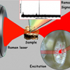
Graphene single-layer flakes were located within ion-bombarded areas with a known defect density and size, using a combination of optical microscopy and Raman spectroscopy. Raman spectroscopy (LabRAM HR Evolution, Horiba Scientific, UK) was performed on these flakes using a 532 nm (2.33 eV) laser source with a total laser spot power of less than 1 mW so that the measurement technique used to determine the disorder in the graphene lattice did not itself create further defects. Raman spectra were obtained for several flakes for each value of LD, for the three types of ion bombardment.
 Raman spectra obtained with a 532 nm excitation laser for Mn ion-bombarded graphene. There is no D-peak present for pristine graphene and the evolution of the D-peak is clearly shown for decreasing LD. Spectra are shown offset vertically for illustrative purposes. (b) D-peak to G-peak ratio (ID / IG) versus the inter-defect distance, LD, for Mn+ (black squares), Bi+ (red triangles) and Bi3+ (blue circles) bombarded graphene. The approximate transition point from Stage 1 to Stage 2 is denoted in (b) by a dashed vertical line and coloured accordingly for each type of ion bombardment, for the specific case of the dashed black line for Mn+ ions, Stage 1 and Stage 2 are annotated. Adapted from Reference 10.")
Figure 2(a) shows the evolution of the single-layer graphene Raman spectra with decreasing average inter-defect distance, LD, (that is, increasing defect density, n) for 25 keV Mn+ ion bombardment, where the value of LD is estimated from 1 / Ön. Pristine single-layer graphene shows the characteristic Lorentzian G- (~1585 cm–1) and 2D-peaks (~2700 cm–1), but as disorder is introduced into the graphene lattice in the form of vacancy defects, a D-peak, at ~1350 cm–1, is activated by the presence of a defect and increases in intensity in relation to the G-peak. The D¢-peak (~1620 cm–1) is also observed for disordered graphene. Depending on the level of disorder in single-layer graphene, the material can be described as Stage 1 for larger values of LD, and Stage 2 for smaller values of LD, as shown in Figure 2(b). For Stage 1, the ID / IG ratio increases with decreasing LD, as the vacancy defects in the sp2-hybridised graphene lattice increase in density. Stage 2 is reached when the average inter-defect distance reaches the point of defect coalescence, and the number of six-atom carbon rings present is substantially reduced and broadening of the G- and D-peaks is observed, as in Figure 2(a) for LD = 0.9 nm. Thus, the broadening of the D-peak can be used to determine whether the level of disorder has reached Stage 2, with the full-width at half maximum of the D-peak greater than ~30 cm–1.10 Figure 2(b) shows how the Raman peak intensity ratio, ID / IG, varies with LD for defects created by bombardment of the three different ions, Mn+, Bi+ and Bi3+.
Equation 18 shows how the defect size (rS) is intricately linked to the quantitative determination of inter-defect distance, LD, where CA is a laser excitation dependent variable, and rA is a length scale that determines the region where the D-peak Raman scattering occurs.

Equation 1 can be used to fit the data in Figure 2(b) where the values of rS were determined using STM. CA and Lσ [the phase breaking length of graphene and equal to (rA – rS) in Equation 1] are kept constant and a good agreement with the experimental data is observed.
From the results of fitting Equation 1 to the three sets of data in Figure 2(b), the parameters CA and Lσ are calculated as 5.0 ± 0.9 (for 2.33 eV laser excitation) and 2.4 ± 0.6 nm, respectively, with a 95% confidence level.10 This level of accuracy and precision is only possible through this investigation of varying LD for several different defect sizes, but enables a much more accurate quantitative determination of both graphene defect density and size for industrial companies using Raman spectroscopy. However, it also experimentally reveals that Equation 1 only allows the quantitative calculation of defect density if the defect size is already known, and vice versa.
Standardisation of graphene
To truly progress from the laboratory to the factory floor, there is a pressing need for international standards in this area. Most urgent is the need for terminology and measurement standards. By defining the terms and nomenclature that should be used, industry can then confidently converse and flourish. Issues such as when does “few-layer graphene” end and “graphite” begin is a typical example that may lead to issues between a supplier and an end-user purchasing material. These terminology issues are being addressed in the “Terminology and nomenclature” Joint Working Group (JWG) within the “Nanotechnologies” Technical Committee of the International Organization for Standardization (ISO/TC229) and TC113 of the International Electrotechnical Commission (IEC), through a standard, ISO/AWI TS 80004–13 “Graphene and related two-dimensional materials”. This document will define the terms associated with graphene and other related two-dimensional materials. This is a crucial first step in the standardisation process to enable other standards to be developed in the same area.
To enable the reliable and accurate measurement of graphene in an industry environment for quality control processes, measurement standards developed by the international community, and validated through metrological investigations and interlaboratory studies, will be required. Several measurement standards are now being developed in JWG2 “Measurement and Characterisation” of ISO/TC229 and IEC/TC113, as well as WG8 “Graphene related materials/Carbon nanotube materials” in IEC/TC113. Through the international standardisation of the measurement of graphene, it will be possible for technician-level employees of companies situated in different parts of the world to characterise commercial material in a way that can be compared globally. However, this process of international standardisation is a rigorous one and thus takes time, with the nominated experts from the member countries contributing and enhancing standards over periods of typically two or more years. For these standards to be as accurate as possible, metrology investigations will be crucial. Investigations such as the one detailed here, determining the relationship between defect size and defect density to allow the truly quantitative measurement of these parameters using a potential quality control technique, Raman spectroscopy.
Conclusions
Raman spectroscopy is a powerful tool for measuring many properties of graphene, including the defect density or defect size, although one of these parameters must be already known to accurately determine the other. The speed of measurement and non-destructive nature of this optical technique will position it as a measurement method of choice for quality control processes. However, the benefit of being able to observe many different types of property changes with this technique, also leads to the issue that any observed change in the Raman spectra may be due to one of several factors. Measurement science investigations into these types of issues will be required to advance this area and enable commercial applications. The calibration of any Raman spectroscopy instrument is typically taken for granted or focused on the accuracy of the spectral position recorded. As shown here, by the need for the determination of the intensity ratio of two peaks and the peak-width of one peak to obtain the level of disorder for graphene, the intensity response function of the detector and the spectral resolution should also be considered.
Techniques such as tip-enhanced Raman spectroscopy (TERS), which provides nanoscale Raman mapping of surfaces, will also further the scientific understanding of the confocal Raman spectroscopy characterisation of graphene. For example, by probing individual nanoscale defects or features, rather than the contribution of many defects due to the micron-scale probe-size of confocal microscopy.
Also, for this technique to be applied on the length-scale and time-scale that will be required for industrial-scale production, the issue of the Raman spectroscopy probe-size (micron-scale) and the typical areas that will be required to measure for chemical vapour deposition (CVD) growth of graphene (metre-scale), will need to be overcome. Possible solutions may be the combination of Raman spectroscopy with other rapid optical characterisation techniques, such as optical microscopy or ellipsometry.
Acknowledgements
The authors would like to acknowledge the Innovation R&D programme of the National Measurement System of the UK Department of Business, Innovation and Skills (Project number 118616).
References
- K.S. Novoselov, V.I. Fal’ko, L. Colombo, P.R. Gellert, M.G. Schwab and K. Kim, “A roadmap for graphene”, Nature 490, 192 (2012). doi: http://dx.doi.org/10.1038/nature11458
- rA.K. Geim and I.V. Grigorieva, “Van der Waals heterostructures”, Nature 499, 419 (2013). doi: http://dx.doi.org/10.1038/nature12385
- Graphene Markets, Technologies and Opportunities 2014–2024. IDTechEx (2014).
- A.C. Ferrari et al., “Science and technology roadmap for graphene, related two-dimensional crystals, and hybrid systems”, Nanoscale 7, 4598 (2015). doi: http://dx.doi.org/10.1039/C4NR01600A
- rA.C. Ferrari and D.M. Basko, “Raman spectroscopy as a versatile tool for studying the properties of graphene”, Nat. Nanotechnol. 8, 235 (2013). doi: http://dx.doi.org/10.1038/nnano.2013.46
- F. Tuinstra and J.L. Koenig, “Raman spectrum of graphite”, J. Chem. Phys. 53, 1126 (1970). doi: http://dx.doi.org/10.1063/1.1674108
- M.M. Lucchese, F. Stavale, E.H. Martins Ferreira, C. Vilani, M.V.O. Moutinho, R.B. Capaz, C.A. Achete and A. Jorio, “Quantifying ion-induced defects and Raman relaxation length in graphene”, Carbon 48, 1592 (2010). doi: http://dx.doi.org/10.1016/j.carbon.2009.12.057
- L.G. Cancado, A. Jorio, E.H.M. Ferreira, F. Stavale, C.A. Achete, R.B. Capaz, M.V.O. Moutinho, A. Lombardo, T.S. Kulmala and A.C. Ferrari, “Quantifying defects in graphene via Raman spectroscopy at different excitation energies”, Nano Lett. 11, 3190 (2011). doi: http://dx.doi.org/10.1021/nl201432g
- P. Blake, E.W. Hill, A.H. Castro Neto, K.S. Novoselov, D. Jiang, R. Yang, T.J. Booth and A.K. Geim, “Making graphene visible”, App. Phys. Lett. 91, 063124 (2007). doi: http://dx.doi.org/10.1063/1.2768624
- A.J. Pollard, B. Brennan, H. Stec, B.J. Tyler, M.P. Seah, I.S. Gilmore and D. Roy, “Quantitative characterization of defect size in graphene using Raman spectroscopy”, Appl. Phys. Lett. 106, 253107 (2014). doi: http://dx.doi.org/10.1063/1.4905128