
Cornelia Streeck,a Thomas Wirth,b Wolfgang Ungerb and Burkhard Beckhoffa
aPTB—Physikalisch-Technische Bundesanstalt, Abbestr. 2–12, 10587 Berlin, Germany. E-mail: [email protected]
bBAM—Bundesanstalt für Materialforschung und -prüfung, Unter den Eichen 87, 12205 Berlin, Germany
In this article the question of the certification of calibration samples for the characterisation of advanced thin film materials is addressed within the framework of reliable process control or quality management purposes. Reference measurement techniques can be used in order to address the gap in appropriate certified reference materials (CRMs) for thin film analyses. They allow for qualifying out-of-production samples originating from an operating production line as calibration samples. As a template for this procedure, CIGS [Cu(In,Ga)Se2] layers, that are absorber layers for high efficiency thin-film solar cells, have been used for establishing and validating reference-free X-ray fluorescence (XRF) analysis and Auger-electron spectroscopy (AES) as reference measurement techniques. The focus was on determining the average mole fractions in the CIGS layers obtaining results traceable to the SI unit system. Reference-free XRF is physically traceable and is based upon radiometrically calibrated instrumentation and knowledge of atomic fundamental data. Sputter-assisted AES can be established as a chemically traceable method after careful calibration using a certified reference material (CRM) based on a total number counting method.
Introduction
To address the challenges associated with energy generation, storage and transfer in the 21st century, innovations in the field of advanced thin film materials need to be transferred as directly as possible into the production process to ensure a fast lane of technological developments. Complex thin films have to be accurately manufactured with respect to their spatial and elemental composition, interface properties and thicknesses. The reliable analyses of these properties is important in the development and production of advanced thin films and is primarily based on dedicated calibration samples being used in the laboratory, in-line or on-line process control.
In general, a prerequisite for an appropriate calibration of complex samples is the similarity of the spatial and elemental structure of the calibration sample to the samples to be analysed. With increasing deviations of the sample composition or thickness between both, an increasing difference between the analytical values derived and the true values are induced due to non-linear matrix effects associated, for example, with (X-ray) absorption, secondary enhancement effects by electrons or characteristic photons or sputtering rate variations. The limited number of available CRMs that can be used as calibration samples for thin film analyses at the nanometre and micrometre scale means there is an important gap in the growing market for novel thin film materials.
In general, calibration samples have the role of an independent reference with respect to the location, measuring device and environment. They globally ensure the reliability and reproducibility of measuring results. Furthermore, CRMs for calibration enable the adherence of strict tolerance limits to improve the profitability of production processes. An important point in quality management systems that meet the requirements of ISO/IEC 17025 is the traceability of routine test results and their validation. This can be achieved by using known calibration samples, e.g. CRMs (chemical traceability), in addition to Round Robin activities for validation purposes. An alternate route is offered by first principle methods that are directly traceable to the measurement units of the SI (physical traceability). Both physical and chemical traceability is considered to be equivalent. Reference-free X-ray fluorescence (XRF) and sputter-assisted Auger-electron spectroscopy (AES) were established for the application of different traceability chains.
Advanced thin film material CIGS
CIGS layers can be considered as a suitable example for a class of thin films that are already in the industrial production processes; but where no appropriate CRMs are available for reliable process control or quality management purposes. CIGS is an abbreviation for the elements present in the layers: copper Cu, indium In, gallium Ga and selenium Se (or sulfur S). The CIGS layers are used as absorber layers for thin film solar cells where their functionality is defined by their spatial and elemental composition. In Figure 1, a typical structure of such a solar cell is depicted. The approximate 2 µm thick layers can reach energy conversion efficiencies over 20%, playing in the same league as multicrystalline Si.1 Both the average composition of the overall CIGS layer and the elemental depth profile of CIGS absorber layers are major factors for determining the conversion efficiency of the solar cell.
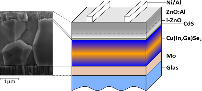
Figure 1. Illustration of a thin film solar cell based on a CIGS [Cu(In,Ga)Se2] absorber layer. On a substrate (e.g. glass) a molybdenum (Mo) layer is used as back contact. The p-type CIGS layer forms the pn-junction with the n-type buffer layer (CdS) and the n-type window layer (ZnO:Al). The photo current can be collected with a metallic grid on top (Ni/Al).
One challenge posed by this sample system is the analytical question of determination of the in-depth elemental gradient. A detailed study on this topic has been published by Abou-Ras,2,3 demonstrating that several methods reveal comparable results within their given uncertainties for the measured gradient, while other methods differ significantly, thus leaving the question of the “true” in-depth gradient somewhat unanswered. The analytical objective of the average composition of the CIGS-layer was addressed as a priority. At PTB, the National Metrology Institute of Germany, and BAM, the German Federal Institute for Materials Research and Testing, reference-free XRF analysis and sputter-assisted AES were set up as traceable measurement capabilities for the characterisation of CIGS layers (see Figure 2).
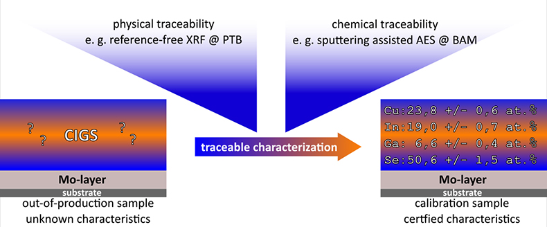
Figure 2. The scheme illustrates the certification of a typical out-of-production sample, here as an example, a CIGS-layer on a molybdenum coated substrate, to a traceable sample for calibration of methods used for in-line analysis at production facilities. The reference measurement methods can be based either on physical or chemical traceability chains.
Reference-free X-ray fluorescence analysis
Conventional XRF analysis is well suited to thin film analysis. About 25% of the world-wide XRF market volume is correlated to analytics of thin layers and coatings. With XRF, the mass deposition of elements can be non-destructively determined. Knowing the density of the thin film, the layer thickness can be calculated, too. The employed XRF devices are quite variable with respect to their size, beam geometry or automation. For conventional quantification, as used on XRF instruments in field laboratories in industrial or scientific applications, they have to rely on a calibration procedure, which is most appropriate when using a dedicated calibration sample similar to the layer to be analysed. The reliability of analytical results here can be considerably improved when using certified thin film calibration samples. Reference-free XRF is a powerful tool for certification of such calibration samples.
The approach of reference-free XRF enables an advanced quantification without the need for any calibration samples. This method is physically traceable to the SI unit for the amount of substance, the mol. It uses well-defined monochromatic radiation, radiometrically calibrated instrumentation and knowledge on atomic fundamental parameters such as interaction cross-sections and fluorescence yields4 (see Figure 3). The measured count rates of characteristic XRF lines per incident radiation intensity from a thin film sample are translated into a mass deposition of the corresponding elements in the film on the substrate.4
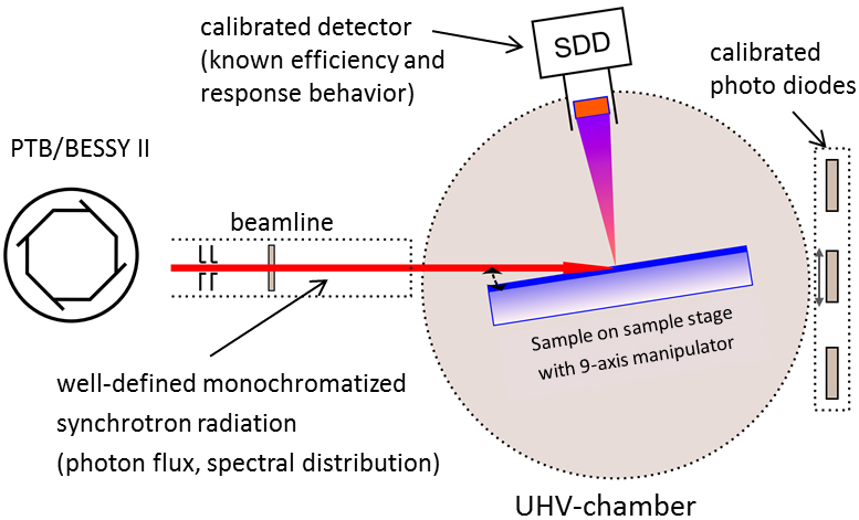
Figure 3. Scheme of reference-free XRF. For XRF spectrometry, monochromatised synchrotron radiation from the soft to hard X-ray range can be used. A solid state detector (SDD) is typically used as the X-ray detector.
A typical XRF spectrum of a CIGS thin film sample for an excitation energy of 11 keV and a calibrated energy-dispersive silicon drift detector (SDD) is shown in Figure 4. The deconvolution of the spectrum is based upon both detector response functions and physical models for background contributions such as X-ray resonant Raman scattering or bremsstrahlung.
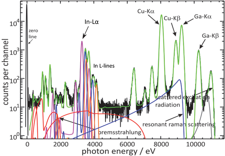
Figure 4. XRF spectrum for a CIGS thin film sample measured at PTB in the synchrotron radiation facility BESSY II for certification of the integral film composition. Cu-Kα, Ga-Ka and In-Lα fluorescence line intensities were used.
Quantification is based on a least-square algorithm fitting measured and calculated fluorescence line intensities. The average composition can be determined by using the typical, standard 45° XRF geometry, for both the angle of incidence and detection. Even the in-depth elemental gradient of a CIGS layer is accessible by using a set of angles of incidence from the shallow grazing incidence regime beginning at about 0.2° up to 45° and fitting the parameters of an appropriate elemental in-depth profile.5
Sputter-assisted in-depth analysis by Auger electron spectroscopy
AES is often used for chemical and compositional analysis of technical surfaces. Due to the small inelastic mean free path of the electron beam induced Auger electrons in the material, the information depth of AES is within few atomic layers. For an analysis of overlayers up to thicknesses of some µm, AES can be combined with argon ion sputtering, enabling elemental in-depth analysis.
At BAM, a PHI 700 Scanning Auger Probe (ULVAC-PHI Inc.) equipped with a cylindrical mirror analyser is used for thin film analysis. Depth profiling was carried out by sequential 3 keV Ar+ ion sputtering. A typical AES survey spectrum of CIGS is shown in Figure 5 together with depth profiles of the elements. For excitation of the CIGS surface layer, a primary electron beam of 5 keV was used.
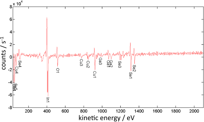
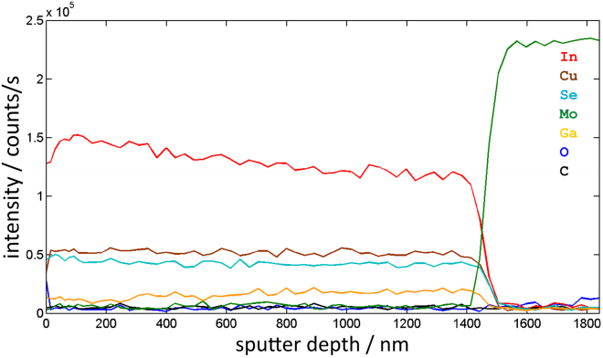
Figure 5. Left: AES spectrum of a CIGS surface after removal of surface oxides and contamination by Ar+ sputtering. Elements are identified by the characteristic kinetic energy of Auger electrons. For the determination of the composition, the Auger transitions Cu LMM (922 eV), In MNN (405 eV), Ga LMM (1070 eV) and Se LMM (1311 eV) are used. Right: elemental depth profile across the CIGS film sample down to the Mo substrate. See text for further details.
The intensity scale of Figure 5 can be expressed in composition data (at.%) when a calibration sample is available. Because CIGS is a quaternary crystalline material, substantial matrix effects in AES have to be expected. Therefore, the composition of such a reference material must be very similar to that of the sample to be measured. The use of a reference material which is certified in a way that its composition is traceable to the SI unit of the amount of substance (mol) would make, by careful calibration, AES a traceable method, too. Options to certify CIGS as reference material are, e.g., ID ICP-MS (isotope dilution inductively coupled plasma mass spectrometry) or reference-free XRF. For layers where the constituents are homogeneously distributed in depth for both the reference material and the sample to be analysed, quantification is enabled by individual elemental sensitivity factors. For CIGS layers with the typical variation of in-depth elemental composition, a quantification of the average composition can be accomplished by a total number counting method. This method is based on measuring the integrated intensity of a constituent element in a depth profile of a similar CRM and a calculation of respective sensitivity factors.6 The signal intensities of the constituent elements are determined from the summation of the individual intensities over all measurement cycles by using either the peak areas or the peak-to-peak heights. This method relies on a CRM and was recently validated by an inter-laboratory comparison organised by an international working group of the International Meter Convention.6
International inter-laboratory key-comparison for CIGS thin films
Both methods, reference-free XRF and sputter-assisted AES with a total number counting method, were part of that key comparison with the objective to compare the equivalency of participating institutes for measuring the average mole fractions of Cu, In, Ga and Se in an approximately 2 µm thin CIGS film.6 The main focus was on sputter-assisted methods. In addition to AES, X-ray photoelectron spectroscopy (XPS) and secondary ion mass spectrometry (SIMS) were also used to determine the average composition of a CIGS thin film by using the total number counting method and a certified sample for calibration. This sample was certified by ID-ICPMS.7 Although AES, XPS and SIMS are not traceable measurement methods on their own, the key comparison has shown that after careful calibration with a certified reference material, traceability is reached. The only method included in the key comparison which does not need the reference sample is reference-free XRF, because it is a primary method with intrinsic traceability.
Summary and outlook
By using reference-free XRF, a primary method with traceability to the SI units mol and metre, determination of the mass deposition of layered samples is possible. The method allows for the determination of average mole fraction and thickness of the layer. Thus, out-of-production samples, exemplarily shown here on a CIGS thin film layer, can be certified as calibration samples for process control by field XRF instruments and other methods like AES, SIMS and XPS. In this way these methods become traceable. Such traceability promotes the value of these methods in quality management systems in test laboratories working under ISO/ICE 17025 accreditation. Moreover, for selected sample systems it could be shown that this XRF methodology is enabling a determination of elemental in-depth gradients.5 However, higher measurement and data reduction efforts are required to reach this goal. The given approach to certify an out-of-production sample in a way traceable to the SI is not limited to CIGS but can also be extended to other types of thin-film sample systems at the nanometre or micrometre scales. Reference methodologies, such as reference-free XRF and calibrated AES, can meet the growing demand on well-characterised thin film samples.
With respect to XRF analysis, a widely used technique in testing laboratories engaged in thin-film analysis, standardisation under ISO/TC 201/SC10 is on-going. The aim is here to establish an ISO standard for the certification of out-of-production samples for thin film analyses by traceably calibrated commercial XRF instruments.
References
- M.A. Green, Y. Hishikawa, W. Warta, E.D. Dunlop, D.H. Levi, J. Hohl-Ebinger and A.W.H. Ho-Baillie. “Solar cell efficiency tables (Version 50)”, Prog. Photovoltaics: Res. Appl. 25(7), 668 (2017). doi: https://doi.org/10.1002/pip.2909
- D. Abou-Ras, R. Caballero, C.-H. Fischer, C.A. Kaufmann, I. Lauermann, R. Mainz, H. Mönig, A. Schöpke, C. Stephan, C. Streeck et al., “Comprehensive comparison of various techniques for the analysis of elemental distributions in thin films”, Microsc. Microanal. 17(5), 728 (2011). doi: https://doi.org/10.1017/S1431927611000523
- D. Abou-Ras, R. Caballero, C. Streeck, B. Beckhoff, J.-H. In and S. Jeong, “Comprehensive comparison of various techniques for the analysis of elemental distributions in thin films: additional techniques”, Microsc. Microanal. 21(6), 1644 (2015). doi: https://doi.org/10.1017/S1431927615015093
- B. Beckhoff, “Reference-free X-ray spectrometry based on metrology using synchrotron radiation”, J. Anal. At. Spectrom. 23(6), 845 (2008). doi: https://doi.org/10.1039/b718355k
- C. Streeck, S. Brunken, M. Gerlach, C. Herzog, P. Hönicke, C.A. Kaufmann, J. Lubeck, B. Pollakowski, R. Unterumsberger, A. Weber, B. Beckhoff, B. Kanngießer, H.-W. Schock and R. Mainz, “Grazing-incidence x-ray fluorescence analysis for non-destructive determination of In and Ga depth profiles in Cu (In,Ga)Se2 absorber films”, Appl. Phys. Lett. 103(11), 113904 (2013). doi: https://doi.org/10.1063/1.4821267
- K.J. Kim, A.S. Kim, J.S. Jang, J.K. Suh, T. Wirth, W. Unger, V.-D. Hodoroaba et al., “Final report of CCQM-K129 ‘Measurement of Mole Fractions of Cu, In, Ga and Se in Cu(In,Ga)Se2 Films’”, Metrologia 53(1A), 08011 (2016). doi: https://doi.org/10.1088/0026-1394/53/1A/08011
- J.S. Jang, H.H. Hwang, H.J. Kang, J.K. Suh, H.S. Min, M.S. Han, K.H. Cho et al., “Quantitative analysis of Cu(In,Ga)Se2 thin films by secondary ion mass spectrometry using a total number counting method”, Metrologia 49(4), 522 (2012). doi: https://doi.org/10.1088/0026-1394/49/4/522

